Introduction | ||||||||||||||||||
|
Everything's gone digital. Digital devices are everywhere. But, what is digital, really? Believe it or not, it's all based on a very few really basic math-like operations on the most basic of numbers - ones and zeros, aka binary. I'm sure you've heard this before, and it tells you nothing. | ||||||||||||||||||
Binary numbers, useless for any ordinary purpose, can be represented electrically, which is the basis of all digital electronic devices, including computers, microprocessors and microcontrollers. A single binary number (either a 1 or a 0), known as a bit, is represented in electrical circuits as being either "On" or "Off", much like the common household light and wall switch. This On/Off state can be stored in an electronic latch or 1-bit memory cell, making the bit a small piece of information. Nearly useless by itself, a single bit as an indicator light (for example) can nonetheless mean something--maybe something important, like "Reactor Meltdown", "Coolant Overtemp", or "Check Engine". But why stop at just one bit? Multiple bits grouped together form unique patterns of ones and zeros and represent many codes, messages and numbers for all kinds of math and general arithmetic computations. One such code group is the byte, composed of 8 bits. There are 256 different combinations of ones and zeros possible with eight bits. Standardized byte codes are used to represent alphabetic characters and small numbers, but meanings designers have assigned to specific 8-bit patterns for specific purposes are limitless. And why stop at 8? Bits can be grouped in any number. Maybe you've heard of a PC computer having a 32-bit processor or a 64-bit processor? These larger groupings of bits are often called words. The number of bits in a word is characteristic of a specific computer and is refered to as its word size. But a byte is always 8 bits. Below is a diagram of a byte. Let's name the 8 bits D0 through D7, "D" for "data". We'll also assign a numeric value to each bit, starting at 1. You know this one... 1+1 is 2, 2+2 is 4, 4+4 is 8, 8+8 is 16, etc. This is kid's stuff easy:
Example: 8 Bits by Name and Value |
The World of Numbers |
To further understand our byte as a number, consider first this ordinary number: |
9527 |
|
Without even thinking about it, you understand the magnitude and structure of the number above: (9 * 1,000) + (5 * 100) + (2 * 10) + (7 * 1) = 9,527 Since there are 10 possible numbers, 0-9, for each digit, a digit's value is ten times greater than the digit to its right. Binary is no different at all. Have a look: 10110Applying the same structure and rules: (1 * 16) + (0 * 8) + (1 * 4) + (1 * 2) + (0 * 1) = 22 Since there are 2 possible numbers, 0 and 1, for each digit, a digit's value is two times greater than the digit to its right. |
Conclusion:To us, ordinary base 10 numbers are much easier to comprehend, visualize, use, and compute in our brains. Not so for our electronic technology. Digital circuits are either on or off, so they convey to other digital circuits only these two states. But, thanks to micro miniaturization, incomprehensible numbers of digital circuits are interconnected to deliver complex functionality at the speed of electricity. But wait! Let's not get ahead of ourselves! |
Logical AND Function
Consider this simple circuit: A battery (left symbol) connects to a light bulb (right symbol) through two on/off switches (top symbols) S1 and S2, wired in series. Unbroken lines are ordinary wires.
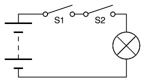
Light is on only if switch S1 AND switch S2 are closed.
Both switches shown in the open (or off) position.
S1 and S2 are ordinary toggle switches, turned on and off by hand. "AND" Logic says that if A (S1) AND B (S2) are on, or TRUE in logic parlance, then we get what we want--a lit-up light. Think of this as a TRUE result. If either switch is turned off--goes FALSE, the light turns off. A dark lamp would be considered a FALSE result. These are the rules of AND.
A digital version of this S1 and S2 circuit (below, left), called a 2-input AND Gate, is switched on or off by voltage (or lack thereof) applied to its A and B inputs. Once the input conditions have been met, that is, both A AND B have the "ON" level (aka "digital 1") voltage, the output Q "goes high" (outputs a "digital 1" voltage) to signify a TRUE or "digital 1" result. No voltage output is a "digital 0" or FALSE result.
Instead of (or in addition to) add, subtract, multiply and divide, digital logic circuits deal in AND, OR, NOR, NOT, NAND, eXclusive OR (XOR) and other logic functions, where one and one don't necessarily make 2. But, they do calculate TRUE or FALSE by the logic specified in their Truth Tables.
These logical calculations are known as Boolean Math. For extra credit, Google its namesake, George Boole.
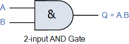
Pictured left is our symbol for a digital electronic AND gate. A and B are logic inputs, while Q is the logic output of the gate. A Truth Table (below) describes its behavior. Remember, 0 is false and 1 is true, where "0" is 0 volts and "1" is, say, 5 volts (though for logic calculations, TRUE and FALSE shall suffice).
| INPUT | OUTPUT | |
|---|---|---|
| A | B | Q |
| 0 | 0 | 0 |
| 1 | 0 | 0 |
| 0 | 1 | 0 |
| 1 | 1 | 1 |
AND Gate Truth Table
If A AND B are true, then Q is true.
Logical OR Function
Here's another one: A logical OR gate (along with an equivalent switch circuit underneath). Turning on switch A OR switch B allows voltage to flow out to Q:
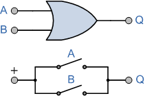
2-input OR Gate
| INPUT | OUTPUT | |
|---|---|---|
| A | B | Q |
| 0 | 0 | 0 |
| 1 | 0 | 1 |
| 0 | 1 | 1 |
| 1 | 1 | 1 |
OR Gate Truth Table
If either A OR B is true, then Q is true.
Now, imagine if, instead of a single gate, we had 5 AND gates lined up side-by-side. All identical, but each gate independent of the others. Five gates equals 5 binary outputs. There are 32 combinations of on and off states possible with 5 bits. All off would be zero, all on would be 31.
Also, there'd be 10 inputs, 5 "A" and 5 "B" inputs for two different 5-bit numbers to AND together. Numbers are coded as described in "The World of Numbers" above.
Here are some 5-bit binary numbers and their decimal equivalent:
| Bit: | D4 | D3 | D2 | D1 | D0 |
|---|---|---|---|---|---|
| Value: | 16 | 8 | 4 | 2 | 1 |
| 1: | 0 | 0 | 0 | 0 | 1 |
| 2: | 0 | 0 | 0 | 1 | 0 |
| 3: | 0 | 0 | 0 | 1 | 1 |
| 4: | 0 | 0 | 1 | 0 | 0 |
| 9: | 0 | 1 | 0 | 0 | 1 |
| 11: | 0 | 1 | 0 | 1 | 1 |
| 22: | 1 | 0 | 1 | 1 | 0 |
| 29: | 1 | 1 | 1 | 0 | 1 |
5-bit And/Or Boolean Math Examples
SOLVE: 11 & 22 (Eleven AND Twenty-Two)
- Step 1: Convert decimal numbers to binary
- Step 2: Line-up binaries vertically
- Step 3: AND together by column each pair of bits for the result
| Value | 16 | 8 | 4 | 2 | 1 |
|---|---|---|---|---|---|
| 11: | 0 | 1 | 0 | 1 | 1 |
| 22: | 1 | 0 | 1 | 1 | 0 |
| &= 2 | 0 | 0 | 0 | 1 | 0 |
This is not unlike a 3rd grade math exercise. Instead of adding or subtracting, we're ANDing: If both bits in a column are 1, the result is 1. If either bit is a 0, the result is 0. Convert the result back to decimal by adding together all "Value" numbers (in yellow, top row) that have a "1" bit in the result. Since only the "2" bit is set, this answer is 2.
SOLVE: 9 | 21 (Nine OR Twenty-One)
- Step 1: Convert decimal numbers to binary
- Step 2: Line-up binaries vertically
- Step 3: OR together by column each pair of bits for the result
| Value | 16 | 8 | 4 | 2 | 1 |
|---|---|---|---|---|---|
| 9: | 0 | 1 | 0 | 0 | 1 |
| 21: | 1 | 0 | 1 | 0 | 1 |
| |= 29 | 1 | 1 | 1 | 0 | 1 |
OR operation: If either bit is 1, the result is 1. Then, add together all "Value" numbers (in yellow, top row) that have a "1" bit in the result.
(1 * 16) + (1 * 8) + (1 * 4) + (0 * 2) + (1 * 1) = 29
Exclusive OR (XOR)
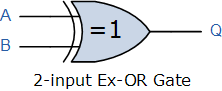
Exclusive OR, or XOR, is a variation of the OR gate. Its output is true if its two inputs are different. If they're the same, whether both true or both false, the result is false. Here's its Truth Table:
| INPUT | OUTPUT | |
|---|---|---|
| A | B | Q |
| 0 | 0 | 0 |
| 1 | 0 | 1 |
| 0 | 1 | 1 |
| 1 | 1 | 0 |
XOR Gate Truth Table
If A is different than B, Q is true.
NOT Gate
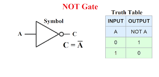
Also called an inverter, its output is the opposite of its input. In its symbology, the actual inverting component is the small circle on the output (C) side of the triangle, not the triangle itself. This "dot" can be added to the output side of any of the above logic symbols, inverting its result. This turns the AND into a NAND, an OR into a NOR, and the XOR into XNOR.
NOT is a logical expression, not an arithmetic function. In binary, if a bit is NOT a zero, then it's a one, and vice-versa. Arithmetically, NOT is ambiguous: For example, while it's true that 522 is NOT 468, saying so doesn't tell you anything about what it is. An analog to this in human reasoning is trying to prove a negative argument. So to digitally invert numbers, we compute a Complement, or CPL, also called a 1's complement.
SOLVE: ~ 11 (CPL 11) = 20. This is an arithmetic verson of NOT
- Step 1: Convert decimal number to binary
- Step 2: Invert each bit to the opposite state (ie, NOT)
- Step 3: Convert the new number back to decimal.
| Value | 16 | 8 | 4 | 2 | 1 |
|---|---|---|---|---|---|
| 11: | 0 | 1 | 0 | 1 | 1 |
| ~= 20: | 1 | 0 | 1 | 0 | 0 |
| += -1: | 1 | 1 | 1 | 1 | 1 |
This is a 1's complement. A number added to its 1's complement always equals -1. But here, 11+20 = 31 with all 5 bits set. What gives? This is not a -1.
This result is only taken to mean 31 as an unsigned integer. But we're expecting a negative result, so we must declare our 5-bit register as a signed integer. The 5 bit pattern remains the same but the recognized number, if negative, is different.
As a signed integer, our most significant bit, instead of having its usual value of 16, is instead a sign flag. If set, the number is negative and the remaining bits are a count-down below zero.
Unary Operators
Unary Operators operate on only one operand, as opposed to binary operators that use two inputs to produce a result. The NOT operation is an example of a unary operator, whereas the AND, OR, and XOR are binary operators. Here are a few more unary functions:
- INC: Increment: Adds 1 to the operand. Symbol: ++
- DEC: Decrement: Subtracts 1 from the operand. Symbol: --
- CPL: One's Complement: Invert all bits. Symbol: ~
- NEG: Two's Complement: Change the sign. Symbol: -
- SHL: Shift Left: Shift bits to the left. Symbol: <<
- SHR: Shift Right: Shift bits to the right. Symbol: >>
- NOT: Logical inverse. Symbol: !
- NOP: No Operation: Does nothing at all.
NOP?? Does nothing? Really? Sure! A NOP in functions is like a zero in numbers. One problem the Romans had with their Roman Numerals: There was no such thing as a zero. This oversight eventually cost them their empire.
SOLVE: INC 31
| Value | C | 16 | 8 | 4 | 2 | 1 |
|---|---|---|---|---|---|---|
| 31: | 1 | 1 | 1 | 1 | 1 | |
| ++ | 1 | 0 | 0 | 0 | 0 | 0 |
In digital electronics, multi-bit unary ops are performed by more complex circuits like registers and ALUs (Arithmetic Logic Units). This example uses a 5-bit counter and introduces the Carry Bit. At 31, our 5-bit counter is at its maximum value, much like an odometer at 999,999 miles. One more increment and it overflows to zero, which is our answer here.
When a counter overflows, it outputs a Carry Bit that, if connected, causes another counter to increment a more significant digit--like 9 incrementing to 10 "carries the 1" to the "tens" place. In decimal or binary, we "carry the 1" while adding (or incrementing) numbers.
SOLVE: DEC 0
| Value | B | S | 8 | 4 | 2 | 1 |
|---|---|---|---|---|---|---|
| 0: | 0 | 0 | 0 | 0 | 0 | |
| - - | 1 | 1 | 1 | 1 | 1 | 1 |
A counter, a common digital circuit, is capable of this, though it is more likely an operation performed by an ALU. One number down from zero is -1, and generates a borrow signal to decrement a more siginificant digit counter, if one exists. This example is the reverse operation of the INC 31 example above.
In order to be a -1 instead of 31, though the bits are exactly the same in either case, we must declare this a signed integer. If we do, the most significant bit or MSB is re-assigned to be the sign bit. If set, (ie, = 1) the number is negative. Such a bit of often called a flag, in this case, a sign flag.
Flags can be assigned any meaning and are likened to the flag on a common mail box. Raising the mailbox flag alerts the letter carrier that there is outgoing mail to pick up even if there is no mail to deliver. Remember what I said about assigning a meaning to a bit. The meaning of a flag bit is limited only by one's imagination.
As a signed integer, our 5-bit register becomes a 4-bit register with a sign bit, so it would then have a numeric range of +15 to -16 instead of 0 to 31.
SOLVE: NEG 14 (Make +14 a -14) Procedure: CPL, then INC
| Value | S | 8 | 4 | 2 | 1 |
|---|---|---|---|---|---|
| 14: | 0 | 1 | 1 | 1 | 0 |
| ~ | 1 | 0 | 0 | 0 | 1 |
| ++ | 1 | 0 | 0 | 1 | 0 |
Another name for a negative version of an integer in signed binary is a 2's complement. To make it negative, start with a 1's complement, (see the CPL operator above) then increment once. Notice the sign bit is set. Presto, you have a 2's complement. When added to its former self, you get zero.
Combinations of various logic circuits such as AND, OR, NOT, XOR, NAND, NOR, etc. that provide instant outputs from their given inputs are known as stateless digital logic circuits.
But those that are one way, then require an event or operation to change to a new result, such as INC and DEC are known as sequential digital logic circuits. Some digital signal has to change on que in order for a counter to count up (or down) one number. In fact, counting how many times a digital signal goes from "0" to "1" is exactly what a counter does! It is inherently sequential.
SOLVE: SHL 23 (shift bits one to the left)
| Bit Name: | C | D4 | D3 | D2 | D1 | D0 | |
|---|---|---|---|---|---|---|---|
| Value | X | 16 | 8 | 4 | 2 | 1 | 0 |
| 23: | 1 | 0 | 1 | 1 | 1 | ||
| << | 1 | 0 | 1 | 1 | 1 | 0 |
Shift Left moves all bits one place to the left. A "0" always moves into the D0 position, while the D4 position (in this 5-bit example) is bumped off into oblivion, or into another register's D0 position if one is connected.
23 << produces a result of 14. SHL normally doubles the number shifted and would have done so this time if the lost D16 bit had a D32 spot to catch it.
If shifted left again, our 14 would become 28. A Shift Register is a sequential logic integrated circuit designed to do this job. Of course, an ALU also has this ability.
SOLVE: SHR 17 (shift bits one to the right)
| Bit Name: | D4 | D3 | D2 | D1 | D0 | B | |
|---|---|---|---|---|---|---|---|
| Value | 0 | 16 | 8 | 4 | 2 | 1 | X |
| 17: | 1 | 0 | 0 | 0 | 1 | ||
| >> | 0 | 1 | 0 | 0 | 0 | 1 |
A Logical Shift Right moves all bits one place to the right. A "0" always moves into the D4 position, while the D0 position (in this 5-bit example) is bumped off into oblivion, which could go into another register's D4 position if one was connected. An Arithmetic Shift Right would instead copy the sign flag into the MSB upon shift.
17 >> produces a result of 8. SHR normally cuts the number shifted in half and would have done so this time, except that 17/2=8.5. Since we're dealing with integers, the lost D0 bit, instead of having a value of 1/2, is simply lost.
If shifted right again, our 8 would become 4.
Addition
Adding numbers is no more than a 3rd-grade old-school arithmetic lesson. Obviously, we're not here to learn how to add numbers, but instead, to review how numbers are added. To better understand addition in binary, let's have a detailed look at the procedure of adding familiar decimal numbers:
| S | O | L | V | E |
| 3 | 7 | 5 | ||
| + | 7 | 5 | 9 | |
Start with the right column: 5 + 9 = 14. Write down the 4 and "carry the 1":
| 1 | ||||
| 3 | 7 | 5 | ||
| + | 7 | 5 | 9 | |
| 4 |
14 is 10 + 4, so the 1 appropriately got "carried" to the 10's position. But, now, in the 10's column, we have 3 numbers to add, and this is important as we'll need to be able to handle it when -- you guesed it -- we construct digital circuitry to do this. But not so fast!
1 + 7 + 5 = 13
| 1 | 1 | |||
| 3 | 7 | 5 | ||
| + | 7 | 5 | 9 | |
| 3 | 4 |
Again, we write down the 3 and carry the 1 to the 100's position. Lastly, add up the 100's column. Again, we have an overflow from the previous column:
1 + 3 + 7 = 11
| 1 | 1 | 1 | ||
| 3 | 7 | 5 | ||
| + | 7 | 5 | 9 | |
| = | 1 | 1 | 3 | 4 |
11 is 10 + 1, so we have one last carry digit. With no other arguments to add to, it ends up in the 1000's position in the total: 1,134.
So...how can an electronic circuit add numbers? Hint: It will operate on binary numbers, not decimal.
Before we can even think about using digital electronic circuitry to add numbers, we need to learn to add binary numbers ourselves. Procedurally, it is no different from adding decimal numbers:
| S | O | L | V | E | |
| 0 | 0 | 1 | 1 | 1 | |
| + | 1 | 0 | 0 | 1 | 1 |
Once again, start with the right column: 1 + 1 = 2, or 10 in binary. Write down the zero and "carry the 1":
| 1 | |||||
| 0 | 0 | 1 | 1 | 1 | |
| + | 1 | 0 | 0 | 1 | 1 |
| 0 |
Next, is the big one: 1 + 1 + 1 = 3, or 11 in binary. Write down the 1 and carry the other 1:
| 1 | 1 | ||||
| 0 | 0 | 1 | 1 | 1 | |
| + | 1 | 0 | 0 | 1 | 1 |
| 1 | 0 |
Next, we have 1 + 0 + the carried 1 = 10. Write down the 0 and carry the 1:
| 1 | 1 | 1 | |||
| 0 | 0 | 1 | 1 | 1 | |
| + | 1 | 0 | 0 | 1 | 1 |
| 0 | 1 | 0 |
The last 2 bits are both 1 + 0 + 0 = 1, no carry bits for a change:
| 1 | 1 | 1 | |||
| 0 | 0 | 1 | 1 | 1 | |
| + | 1 | 0 | 0 | 1 | 1 |
| = | 1 | 1 | 0 | 1 | 0 |
Or, in decimal, 7 + 19 = 26. So, what? Boring, right? Sure. But, you understand it, huh? Now the real task: Use this boring exercise and the gates described above to construct digital circuitry that can add numbers. Bet you didn't see THAT coming!
The Truth about Adders
So far we've described a logic circuit and from the way it was defined to work, a Truth Table was made. But now, we'll make the truth table first. We need our Adder circuit to do this:
- 0 + 0 = 0. Duh. But true!
- 1 + 0 == 0 + 1 = 1.
- 1 + 1 = 10, but we keep the 0 and "carry away" the 1.
- We generate a carry when both bits to add are 1's.
- We need two inputs, A and B, and need two outputs, a Sum and a Carry.
Introducing the Adder:
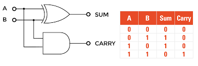
Both gates get the A and B inputs. The XOR gate produces what can be used as a sum, while our handy AND gate just happens to generate the needed carry bit. Trick, huh?
By themselves, these various gates don't do much. But, just like players on a team, when you combine their talents through clever positioning and connections, they quickly become more interesting. Consider it a kind of a puzzle. If you like solving puzzles, digital circuitry just might be for you! And there are SO many more digital team members to get to know! Like the Shift Register, mentioned above.
These basic Small Scale Integration, or SSI gates, are amazingly inexpensive integrated circuits, or ICs and are easy to experiment with using a "Solderless Breadboard" or "Proto Board", available from amazon.com, among other places. Of course, as ICs evolved, their internal part counts exploded, giving us Medium and Large Scale Integration devices. But don't worry! You don't need to understand how to design them, only how use them. No one knows it all! Once a device's function is understood, we need not delve into its internal details.
Honestly, I've had years of fun exploring this stuff, and I'm certainly not alone! Yeah, geeky for sure. But if you can imagine it--once you get to know the "team members"--actual digital integrated circuits perform exactly as envisioned.
Congratulations on your first multi-gate endeavor, the Adder. By arraying multiple adders together, we can add multi-bit numbers. More adders equals bigger numbers.
But wait...there's something missing. We generate a Carry Bit, but we need to be able to add-in a Carry Bit from the adder on the right, and our adder doesn't do this.
Sadly, our adder circuit is really only good for the least-significant bit, or LSB, since it's the only position that doesn't receive a Carry Bit. So let's call it a Half Adder. A new adder circuit needs to be designed to add three bits together: A, B, and a Carry In. Other than that, it would work the same. Here's the Truth Table that would describe our new adder:
FULL ADDER Truth Table:
| INPUT | OUTPUT | |||
|---|---|---|---|---|
| Carry In |
A | B | Sum | Carry Out |
| 0 | 0 | 0 | 0 | 0 |
| 0 | 1 | 0 | 1 | 0 |
| 0 | 0 | 1 | 1 | 0 |
| 0 | 1 | 1 | 0 | 1 |
| 1 | 0 | 0 | 1 | 0 |
| 1 | 1 | 0 | 0 | 1 |
| 1 | 0 | 1 | 0 | 1 |
| 1 | 1 | 1 | 1 | 1 |
Notice the top half of our Full-Adder truth table is the very same as our Half-Adder. The lower half, with Carry In set, has a Carry Out that looks like the output of our OR Gate.
Another observation: Adding two bits, A and B, produce a single bit. Adding this single bit and a Carry In bit is a job for another half adder. If either of these two Half-Adders produce a carry, we'll want a Carry Out bit for the next adder. Hmmm. Either Carry A OR Carry B... Maybe our Half-Adder is not so useless after all.
Full-Adder Circuit
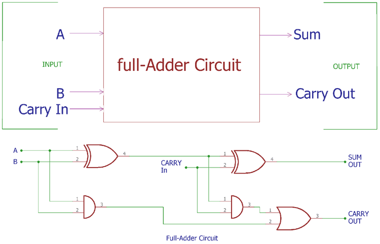
This FULL ADDER is actually two Half-Adders with their Carry Outs OR'd together. Now, we can cascade together as many Full-Adders together for as many bits needed. Excepting that it's in binary, an array of Adders can really add large numbers in a mere instant.
Additional Information Sources
Information about Digital Logic Devices has been published by chip manufacturers in Catalogs, indexed by industry-standard and/or manufacturer specific part numbers. In book form, catalogs typically describes the device's operation and truth tables and are educational just to browse.
Unfortunately, the Internet has all but relegated these informative books to history's dust bin, but most all this information is available online by Googling. Google Images is especially helpful. Still, there's no substitute for flipping pages in a physical book. You just might see something that catches your eye.
Another information source is available online from distributors like Mouser Electronics. Resourceful, yes, but difficult for newbies.
As an exercise, try Googling the integrated circuit part numbers below. Also, you can Google Images for And Gates, Flip Flops, Counters, etc.
- 74LS08 Quad 2-input AND Gate
- 74LS06 Hex Inverter
- 74LS32 Quad 2-input OR Gate
- 74LS86 Quad Exclusive OR Gate
- 74LS00 Quad 2-input NAND Gate
- 74LS10 Triple 3-input NAND Gate
- 74LS74 Dual D-Type Flip Flop
Look for sites that don't require you to install something to view their drawings. There are plenty of sites available that don't. These industry-standard devices have long-since been in the public domain.
Also, there are many, tutorial sites out there that shed light on digital logic basics and beyond. Here's one.
Next: The NAND Gate:
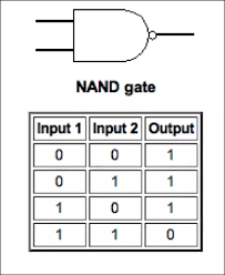
NAND is "Not And", combining the familiar AND Gate with a NOT dot, that open dot on the output line. When both inputs are 1, the output is 0. Recall the AND Gate, the output is 1 when both inputs are 1. NAND has the opposite output response, but other than that, it is the same as the AND.
Or, you could describe the NAND Gate this way: "If either input goes low, the output goes high." NAND Gates appear more frequently in digital circuits than AND Gates. Consider this contraption:
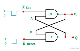
R-S Flip Flop
This one is a brain teaser! Knowing what you know about NAND gates, figure out what happens when input S goes low, then returns to high. Think it through again for when input R goes low momentarily.
Flip Flops
Flip Flops aren't limited to summer footwear. We have 'em too! and there are several variations. The circuit above and to the right is an R-S Flip Flop, sometimes called a Latch, and is the most basic kind of Flip Flop. The very first digital computer was made up of tens of thousands of flip flop circuits, each one built on an individual circuit board. Very early models, long before the invention of the IC, were built using vacuum tubes, which were relatively huge and consumed a whole lot of power when tens of thousands were switched on.
Our R-S Latch is made up of two NAND Gates. Its inputs are R and S for Reset and Set, and its outputs are Q and Q-bar. The "bar" over the top of Q is pronounced "Q-bar", meaning Active Low--that is, it "does its thing" at logic state 0. Also, both R and S inputs are active low.
Each output is connected back to one of the inputs of the opposite gate, leaving the other input (of each gate) to either Set Q High or Reset Q to Low. Once flipped (or flopped?), the circuit remains in state.
OK, let's figure out how this thing works. Assume Q is low. Q is the output of NAND Gate X, so for it to be low, both inputs must be high. This means that Q-bar, the output of NAND Gate Y, must be high, as it is connected to input A of its companion Gate X. Either of Gate Y's inputs can be low to make its output high. This makes sense because we already know input B is low, as it is connected to Gate X's Q output. So now, we're right back where we started.
See what I mean about digital circuitry being like puzzles? I hope you're not puzzled by the above paragraph. Read it a few times until you understand it. It literally teaches you to think!
What's different about the R-S Flip Flop from our description about how a NAND Gate works by itself? Well, nothing, actually. And everything. While it's still true that if both inputs are high, the output of the NAND Gate is low, the R-S Flip Flop will sustain its output state forever until changed by the input receiving a low signal. It "remembers" the "Set" (or "Reset") state long after the inputs have returned to their normally high state.
Basically, we have a 1-bit static memory, and memory is one of the essential things that makes a computer tick. Well, no, actually, it's the clock signal that makes the computer tick. But you catch my drift, yes? So the state of Q, 1 or 0, is the actual data bit of our 1-bit memory unit. We can forget about Q-bar for now. Sometimes it comes in handy where an inverted version of Q is needed.
So, assume Q is low again. Let's pretend the S-bar input to Gate X is connected to a push-button switch. When pressed, the button switch brings S-bar to a temporary low state. A low input on Gate X makes Q high. This makes Gate Y's input B high. Input R is normally high, so with both inputs high, Gate Y's output goes low and stays low. So now, input A on Gate X is low. This is enough to sustain Gate X's output high regardless of what is going on with our push-button switch connected to the S-bar input. Presto! a "clean" flip setting Q high.
Bringing input R low for a moment will reset Q back to the 0 or off state. Input R can then pulse repeatedly low without causing Q to change. This definetly has uses in the real world, not just a one-bit memory. It makes a great switch contact debouncer, for one thing.
Type-D Edge-Triggered Flip Flop
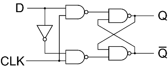
This gadget is called a Type-D Edge-Triggered Flip Flop. Normally, its symbol is a rectangular box which we'll see a little later but for now, it's easier to understand by examining the actual arrangement of its 4 NAND Gates. The good news here is that 2 of these Gates we already understand from the previous discussion of the R-S Flip Flop.
A single 74LS74 integrated circuit contains 2 independent D-Type units and features direct access to the Set and Reset inputs to the R-S Latch, not shown in our basic diagram here.
It may be seem hard at first to justify the existence of this device, but believe me a lot of digital devices use the "Big D". It is definetly a team player!
D is the data input and CLK is a Clock signal. The functional description: "Data present on the D input is transferred to Q on the rising edge of the clock." Of course, Q-bar will always be in the opposite state of Q.
What? Wait...Clock? Whaddya mean Clock?? Does it tell time?
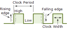
Typical Clock Signal
A clock in this context is a digital signal that cycles between 1 and 0 at a periodic time or at a set rate of speed. Not that the D-Type's CLK input requires such a signal, no. It is called CLocK because it is active upon a transition from a 0 to 1. This is our first foray into sequential logic.
Operational analysis: Assume Q, D, and CLK are zero. Next, we raise D from a 0 to a 1. Note that D is presented to the upper NAND Gate, and D-bar from the inverter goes to the lower NAND Gate. Both input NAND Gates share CLK, and with CLK at zero, the buck stops here. Unless both NAND Gate inputs are high, the output is high, or inactive as far as the R-S section is concerned. You might recall that the R-S Flip Flop's inputs are active low.
OK, lets take CLK high to the 1 state. Since we have D and D-bar both and a NAND Gate for each, one or the other NAND Gate is going to find both inputs high, turning its output low. Whichever one does wins the state of the R-S Flip Flop. It just so happens that if D was high at the time CLK transitioned to high, Q will be the one going high, driving Q-bar low. CLK returns to the low state, and any new changes to D are ignored.
Note: As long as D doesn't change, Q will not change no matter what the clock does.
But wait! What happens if D changes state while CLK is still high? Looks like D will get through an input gate and flip the R-S flop. OOPS! Yup, sure will. Now we must revise our functional description: "Q will follow D as long as CLK is high. Data present on D will be latched on Q upon the falling edge of the clock."
Holy Cow! This isn't a D-Type Edge-Triggered Flip Flop at all. It's a Data Latch. I guess I was a little over-zealous searching for a Flip Flop circuit that was easy to analyze. My bad... Let's fix it!
Remember, our first Adder circuit turned out to be a Half Adder because it was incapable of adding in a Carry Bit? The solution was to use two Half Adders to make a Full Adder. Looks like the solution to our Type-D dilemma is to do the same thing: Add another data latch circuit, per the diagram above.
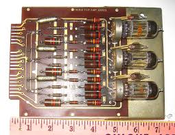
Vacuum Tube Flip Flop from the 1950s
Type-D Edge-Triggered Flip Flop, Take 2
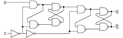
Analyze this!
Assume D, CLK, and Q are all low. In this version of the Type-D Edge-Triggered Flip Flop, CLK is first inverted, so a high is presented to the input NAND Gates. D then flows through to the first R-S latch. Notice the lower input NAND Gate now gets its signal from the upper input NAND Gate, using it as an inverter, thereby making a separate inverter unnecessary. Smart!
So, the first R-S will flip and flop as D changes so long as CLK enables its input NAND Gates. But CLK is inverted again with a second inverter, turning off the input NAND Gates to the right-hand latch, preventing any change of the final Q output. Either the left side input gates are enabled by CLK OR the right side input gates are, but not both.
Finally, let's raise CLK to HIGH. This immediately isolates the left side R-S latch by shutting down it's input gates, then enables the right side input gates. Whatever state the left side R-S latch is in is then carried to the right side R-S latch and Q. No further changes in D can get through until the next rising edge of CLK.
Type-D Flip Flop Divides by 2
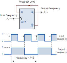
Here's an example of the Type-D Flip Flop in action as a frequency divider. It is also an example of Sequential Logic. Also introduced here is the Timing Diagram, which does for sequential logic circuits what a truth table does for logic gates. And, we're finally diagramming with the rectangular logic symbol instead of the detailed gate diagrams, which simplifies reading by de-emphasizing unnecessary details! Tell you what, we're goin' places now!
The upper Square Wave Pattern labeled Input Frequency is a clock signal oscillating between 0 and 1 logic voltage levels, as marked. It shows 4 rising edges, occuring over an unknown time base, but likely a short length of time. This signal is connected to the Type-D Flip Flop's CLK input. Notice our Q-bar output is connected back to the D input. The lower square wave pattern is produced at the Q output. Let's analyze:
Assume Q-bar and the connected D input are HIGH. CLK and Q are low. When CLK goes high, "data present at the D input is transferred to the Q output", making Q high. (Refer to the Output Frequency square wave pattern above.) Q-bar is always the opposite of Q, so it and D are now low.
This Type-D Flip Flop is a positive edge-triggered device, so nothing happens when CLK goes low. But when CLK turns once again back to the 1 state, D is still low, so Q transitions to low, driving Q-bar and D high. This cycle repeats endlessly. The take-away--Q is changing states every other time CLK rises, so it toggles at half the speed as the clock.
This achieves the divide by 2 function, as advertised! Not an arithmetic divider...in sequential logic, it's a frequency divider. We will see more of this shortly. By the way, the Output Frequency of this device is always a perfect 50% duty cycle, meaning Q is high for the same length of time that it is low.
Integrated Circuit Flip Flop from the 1970s
Let's add three more divide-by-2 Flip Flops: Here we go again: 1+1 is 2, 2+2 is 4... Four Flip Flops divide by 16. But there's more: By bringing out the four Q outputs, we have...
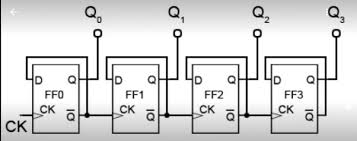
A 4-bit Binary Counter
Lining up the 4 Q's shows what they do in a span of sixteen clock cycles:
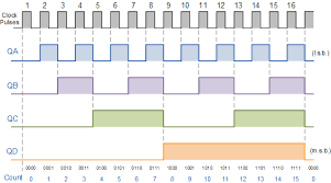
Counter Output Timing Diagram
Here are some more devices to Google:
- 74LS90 Decade Counter
- 74LS93 4-bit Binary Counter
- 74LS160 4-bit Synchronous Decade Counter
- 74LS161 4-bit Synchronous Binary Counter
- 74LS192 4-bit BCD Synchronous Up/Down Counter
- 74LS193 4-bit Binary Synchronous Up/Down Counter
- CD4024 7-stage ripple-carry Binary Counter
- CD4040 12-stage ripple carry Binary Counter
- 74LS47 Seven-Segment Decoder/Driver
- CD4026BE Decade Counter with 7-Segemt Decoder/Driver
- MAX7219CNG 8-Digit Common Cathode Display Driver
Excepting the MAX7219, all these ICs are out of the 1970s and they're still available today. The MAX7219 is a more recent design that takes the place of a dozen or more older chips. I don't expect newbies to completely understand the MAX, but you might get an idea of how ICs have continued to evolve. Without understanding the basic building block of logic, it's far more difficult to get a handle on today's devices.
Binary Counter Truth Table
| Cycle | Q3 | Q2 | Q1 | Q0 |
|---|---|---|---|---|
| 0: | 0 | 0 | 0 | 0 |
| 1: | 0 | 0 | 0 | 1 |
| 2: | 0 | 0 | 1 | 0 |
| 3: | 0 | 0 | 1 | 1 |
| 4: | 0 | 1 | 0 | 0 |
| 5: | 0 | 1 | 0 | 1 |
| 6: | 0 | 1 | 1 | 0 |
| 7: | 0 | 1 | 1 | 1 |
| 8: | 1 | 0 | 0 | 0 |
| 9: | 1 | 0 | 0 | 1 |
| A: | 1 | 0 | 1 | 0 |
| B: | 1 | 0 | 1 | 1 |
| C: | 1 | 1 | 0 | 0 |
| D: | 1 | 1 | 0 | 1 |
| E: | 1 | 1 | 1 | 0 |
| F: | 1 | 1 | 1 | 1 |
A through F? Why not 10-15? Simple! By using a single character to represent 10 through 15, we expand our world of numbers from base 10 decimal to base 16 hexidecimal.
Each hexidecimal digit takes the place of 4 binary bits and is mathematically equivalent. As our digital world expands, more and more bits are needed. To write down or document bit patterns in binary when you're dealing with 8 or 16 or more bits at a whack becomes tiresome and impractical.
So, being true to geekdom, we write in hex. The truth table above is also a binary-to-hex conversion table. But you can do it in your head if you remember our 8-4-2-1 formula from way back in the unary operator section.
Example: Which is more readable: 0111111101011010 or 7F5A? I rest my case. Go Geek!
The Decade Counter
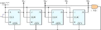
If you took the time to look-up and read-up on the 74LS90, you might already know about the Decade Counter, which divides by 10 instead of 16. So there is hope for base-10 numbers after all! It's called Binary-Coded Decimal or BCD. It would be nice to have counters that count like we do, right? But, how does it work? Refer to the drawing above:
This unit uses J-K Flip Flops. Remember, I said that there were several different kinds of flip flops? Well, here's an example, though I don't think they're used much anymore as discreet circuits, such as the 74LS73. By tying its J and K inputs high (logic 1) it toggles just like a Type D flip flop with Q-bar connected back to D.
Look at the Binary Counter Truth Table above. What a decade counter does, duh, is count from 0 to 9. Upon reaching 10, or "A", a NAND Gate, with its inputs connected to Q1 and Q3, produces a 0 or low output. Instantly (or close to it) the NAND Gate drives all four flop's CLR-bar low, setting all four Q outputs to 0. The NAND Gate returns to the high state and counting resumes at zero.
A counter can drive a 7-segment decoder/driver and a 7-segment display so that we can see the digit. The CD4026B is a decade counter with a 7-segment decoder/driver built in.
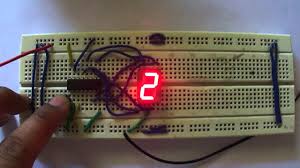
CD4026 Decade Counter/Driver with 7-Segment LED Display
A Proto Board (above) greatly speeds and simplifies experimenting with digital logic circuits and is an inexpensive and fun way to get hands-on experience. Easy to use, too! If you're buying, get a bigger one--proto boards quickly run out of room as your projects grow.
Another thing you'll need is a 5-volt Power Supply to power-up your circuits. An old 5-volt DC wall wart or a USB charger will do fine. Label the wires so you'll always know Positive (+) from Negative (-) DC Polarities. Vcc on these ICs is always positive (+), Gnd negative. Getting these reversed destroys ICs fast.
Life in Seven Segments
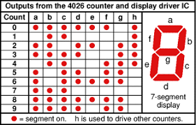
7-Segment Truth Table
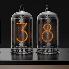
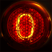
If you've ever wondered how those electronic digits are produced, here's the truthful answer. Obviously, 7-segments are aren't the only way to display. There are also 14-segment displays, dot-matrix units, raster displays, even shaped cold-cathode Neon Nixie Tubes of long ago:
|
|
Cold Cathode Nixie Tubes | |
|
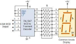
More modern than Nixie Tubes and much less expensive, the ubiquitous 7-segment display is still in use. Diagrammed here is a 74LS47 7-segment decoder interfaced to a LED display through resistors, marked "R". |
Inputs are the 4 Q lines from a 4-bit latch like the 74LS75 or a Decade Counter like the 74LS90. RBO (Ripple Blank Out) and RBI (Ripple Blank In) provide logic to suppress leading and/or trailing zeros in a multi-digit display. Food for thought: Why would you want to use a latch circuit between the counter and the decoder?
Dennis Murphy
February 20, 2020